News
Nepcon Japan
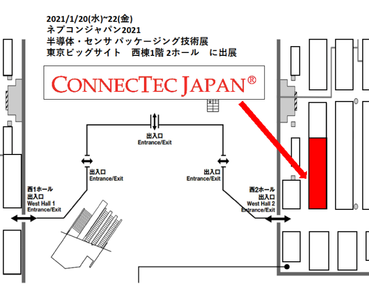
CONNECTEC JAPAN will exhibit at Nepcon Japan (Semiconductor and Sensor Packaging Technology Exhibition) held at Tokyo Big Sight.
■Date and time
From Wednesday, January 20, 2021 to Friday, January 22
10:00 a.m. to 6:00 p.m. (until 5:00 p.m. on the last day only)
■Booth location
Tokyo Big Sight West Building 1F Hall 2 Entrance
At the booth, we introduce the contents and examples of the contract development service “OSRDA” based on our low-temperature low-load bonding technology “MONSTER PAC”, and we will respond immediately to your consultations and questions during the holding period.
In addition, FSNIP*, a narrow pitch wiring forming technology of 40 μm to 10 μm, will be exhibited this time. (*Free Substrate-Material Narrow-Pitch Imprinted Process)
Please do come and see us at our booth.
■Nepcon Japan Special Lecture
Mr. Hirata,CEO is scheduled to give a lecture at the following date and time.
Date: 20th January (Wed.) 10:00am-11:00am