Contract development
OSRDA
OSRDA stands for Outsourced Semiconductor Research Development and Assembly.It is the world’s first business model.
The world’s first business model OSRDA
【Semiconductor Contract Business】 Capable of variable and multi-product assembly

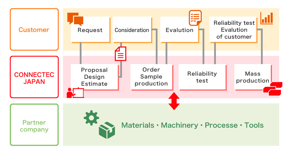
Entrusted Development Service Procedure
We will offer it on a one-stop basis from structure design until sample preparation.
We will totally support your requests from assembling semiconductor chips, MEMS chips, surface mounting, module proto-typing, evaluation/analysis, reliability test, mass-production.
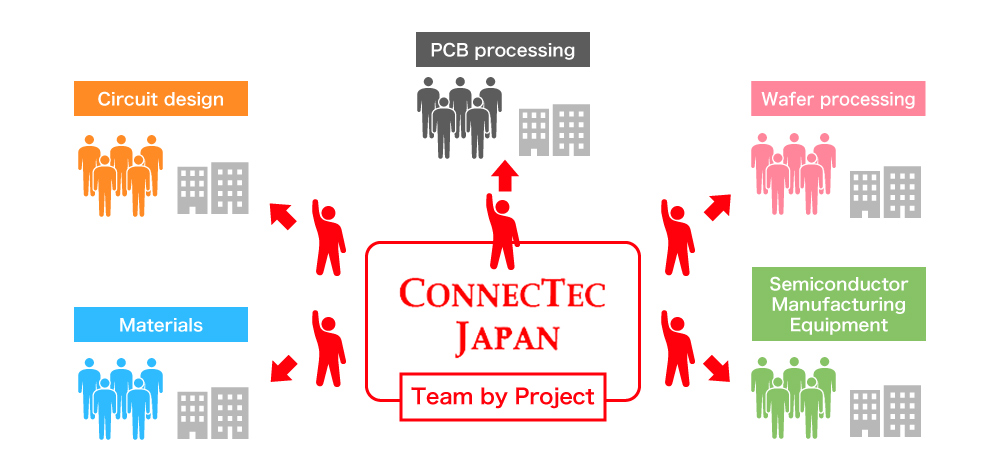
By connecting all the technologies of the Japan, which is the origin of our company name, We provide comprehensive support for semiconductor chip, not only MEMS chip, PCB mounting, module prototyping, sample prototyping, evaluation and analysis, reliability evaluation, and mass production. In cooperation with affiliated companies, research institutes, universities, etc., we provide services to meet your needs.
We will also respond to request from clients in cooperation with our partner companies.
OSRDA From order to mass production

Independent Development
Independent Development
| Concept | Structure/ Process Design |
Trial | Evaluation | Mass Production |
|---|---|---|---|---|
| ○ | ○ | ○ | ○ | ○ |
Entrusted Development
| Concept | Structure/ Process Design |
Trial | Evaluation | Mass Production |
|---|---|---|---|---|
| Customer | ○ | ○ | Consultionl | Consultionl |
Joint Development
| Concept | Structure/ Process Design |
Trial | Evaluation | Mass Production |
|---|---|---|---|---|
| ○/Customer | ○/Customer | ○ | Consultionl | Consultionl |
Trial Manufacture
| Concept | Structure/ Process Design |
Trial | Evaluation | Mass Production |
|---|---|---|---|---|
| ○/Customer | ○/Customer | ○ | Consultionl | Consultionl |
Produce and Promote
Proto-typing Process Menu
Responding to all your requirement, Semiconductor chips and modules, ceramic, organic, film, etc., can be applied to various substrate materials. In addition to the process, we offer a variety of MonsterPAC menu, the process that best suits your needs and implementation structure.
Major Examples of Proto-typing
Semiconductor chips and DRAM, we have been using various substrates such as ceramics, organic, and film to realize the damage-free process of low-temperature low-load, depending on the mounting form of sensors and modules. Please rely on our experienced Connectec Japan.
