Service
Our strength
We serve to design any kind of devices and modules, etc.
We offer ‘one stop R&D’ for device construction proposal, design, process proposal,
Prototype building, reliability testing, and volume production.
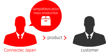
Flow
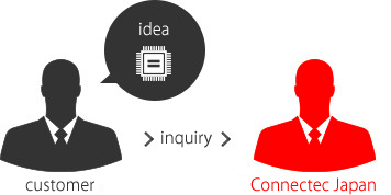
customer/CONNECTEC JAPAN
Please contact us for any implementation requests.

CONNECTEC JAPAN
We provide solutions for customer implementation issues.

- ・dispense
- ・flip chip bonding
new process development
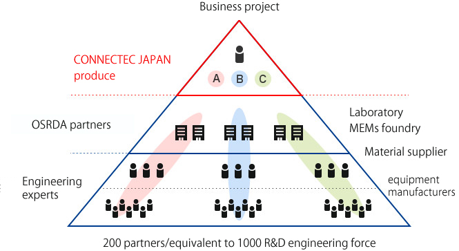
OSRDA
(Outsourced Semiconductor Reserch, Development & Assembly)
Customer
We will introduce various case examples, and you can use products that meet your needs.

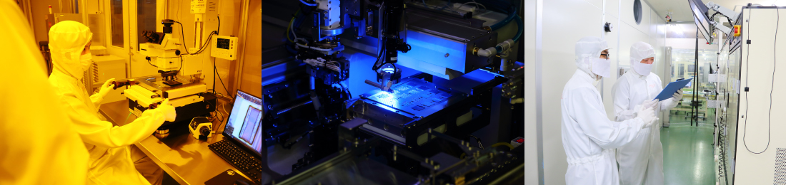
About us
CONNECTEC engineers have
good experience and technologies.
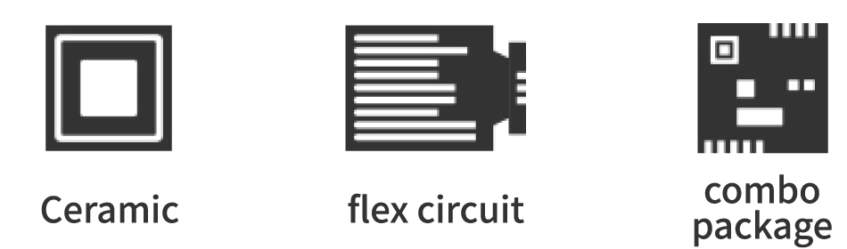
And we have wide selection of substrate materials, i.e. ceramic, organic, film, etc. for various semiconductor devices, DRAM, sensor and module, and build them with low temp./low load ‘damage free’ process.
Produce & promote